Thin-film coating measurement on semiconductor wafers and related substrates can be difficult because the coatings are often very uniform-looking, very thin, and highly sensitive to process variation. In many applications, a few spot checks or rough inspection methods do not provide enough insight into coating uniformity or repeatability.
Small thickness differences can matter when evaluating thin films, protective coatings, and precision process layers.
Contact-based methods are not always desirable when handling delicate substrates or tightly controlled surfaces.
Point-only inspection may not show coating variation across the surface or reveal subtle process drift over time.
Advanced materials and semiconductor teams often need better data for process development, validation, and repeatability studies.
For engineers trying to improve thin-film process understanding, validate coatings without touching the surface, or collect better thickness data, non-contact coating measurement can provide a much more useful workflow.
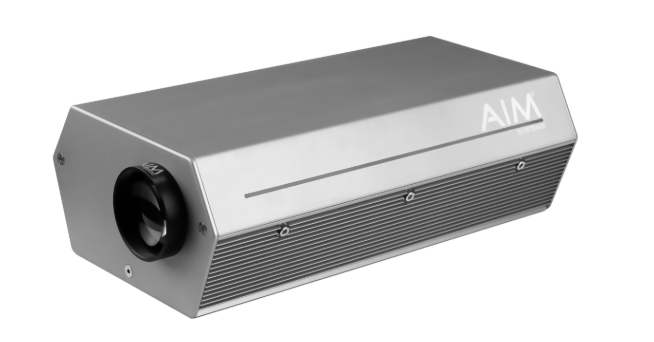
AIM Systems uses a photothermal coating thickness measurement principle to determine coating thickness without contacting the surface. For semiconductor wafers and related thin-film applications, this makes the system attractive where repeatability, surface protection, and non-contact inspection are important.
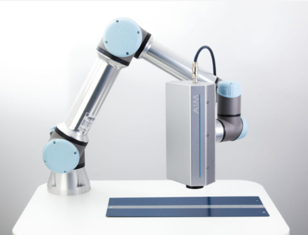
The CoatPro platform can be used in applications where precision coating inspection, process development, or automated measurement workflows are more valuable than simple spot checks. This is particularly relevant for advanced materials, wafer-level coating evaluation, and related electronics process environments.
Ethernet communication, Modbus TCP PLC integration, Power-over-Ethernet, and multiple measurement modes help the system fit into engineering labs, automated inspection cells, and more structured process data workflows.
If your team is trying to move from limited spot measurements toward better thin-film data or mapped inspection, this is the type of architecture worth evaluating.
For a deeper technical explanation of how this measurement method works, see our guide to photothermal coating thickness measurement technology.
| Measurement Principle | Photothermal (non-contact) |
| Typical Substrates | Wafers, advanced materials, coated technical surfaces |
| Coating Type | Thin films, protective coatings, process layers, specialty coatings |
| Measurement Modes | Single-point, continuous scan, mapped inspection |
| Integration | Ethernet, Modbus TCP, PoE |
Semiconductor wafer coating thickness measurement is especially relevant in applications where coating sensitivity, repeatability, process development, or surface protection make manual inspection less attractive. This can be useful for evaluating photoresist thickness, thin protective coatings, and other precision process layers used in semiconductor and electronics manufacturing.
Wafer-related coating processes, specialty thin films, and electronics manufacturing environments where non-contact inspection is valuable.
Engineering teams working on coating repeatability, process setup, and measurement validation on advanced materials.
Thin protective layers and specialty coatings where surface sensitivity and thickness verification are important.
Applications where automation, mapping, and process data are more valuable than simple pass/fail spot checks.
If the goal is better thin-film process understanding, fewer quality escapes, or more confidence in coating repeatability, this category is often worth evaluating.
Convert between coating thickness, coating weight, and density for engineering calculations and specification review.
Estimate the return from improved coating consistency, reduced scrap, better process visibility, and fewer quality escapes.
Review broader coating thickness and coating weight measurement technologies supported across AIM Systems and Scantech applications.
Gauge Advisor is the official sales and service partner for AIM Systems to deliver non-contact coating thickness measurement solutions for demanding production and development environments. AIM’s photothermal systems support thin-film inspection, automated measurement, thickness mapping, and repeatable measurement workflows for advanced coatings and sensitive surfaces.
Send your coating type, typical thickness range, substrate, measurement objective, and whether you need single-point verification, mapped thickness data, or automated inspection. We will help you determine the most practical measurement approach for your application. Not sure whether your coating or surface is a fit? We offer application review and testing support to help assess measurement repeatability.